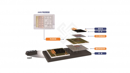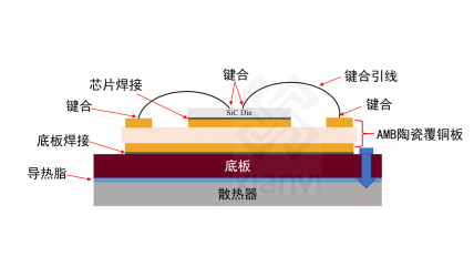


AMB Ceramic Substrates
Active Metal Brazing (AMB) ceramic substrate usually used as the package substrate for high-voltage power devices and it is specially suitable for the package demand of the third-generation semiconductor SiC devices..
Features
lSelf-developed active brazing material
lWhole process flow self-controlled
lUltra-low interface void, high thermal conductivity
lExcellent temperature shock resistant, high reliability
Specifications
Ceramic Specification | Thermal Conductivity (W/m·K) | Si3N4: ≥80 | AlN: ≥170 | ZAT: ≥27 |
Thickness (mm) | 0.25/0.32 | 0.25/0.38/0.63/1.0 | 0.25/0.32/0.38 | |
Copper Specification | Thickness (mm) | 0.3/0.4/0.5/0.8 | ||
Product Specification | Max Dimension (mm) | 138*190 | ||
Max Usable Area (mm) | 127*178 | |||
Product Performance | Void Ratio (C-SAM, 50 um resolution) | <0.3% | ||
Peel Strength (N/mm) @50 mm/min, copper thickness 0.3mm | >10 | |||
Life (cycle) @-55~150℃, holding 15min, transfer <10s | >5000 | >40 | >200 | |
Solderability | >95% | |||
Wire Bonding @300um Al wire, shear speed 500um/s, shear height≤30um | Shear strength≥1000gf Al residue ≥50% | |||
Ceramic/Copper Thickness Combinations
Copper Thickness/mm Ceramic Thickness/mm
| 0.1-0.3 | 0.4 | 0.5 | 0.8 |
0.25 | Si3N4, ZTA | Si3N4, ZTA | Si3N4, ZTA | Si3N4 |
0.32 | Si3N4, ZTA | Si3N4, ZTA | Si3N4, ZTA | Si3N4 |
0..38 | AlN, Al2O3/ZTA | - | - | - |
0.63 | AlN, Al2O3 | AlN, Al2O3 | AlN, Al2O3 | - |
1.00 | AlN, Al2O3 | AlN, Al2O3 | AlN, Al2O3 | AlN, Al2O3 |
Surface Treatment of AMB Ceramic Substrates
Surface Roughness of Copper | Ra≤1.5μm, Ra≤10μm, Rmax=50μm | |
Plate | Bare Copper &Anti-oxidation | - |
Electroless Ni | 2~10μm(P 6%-10%) | |
Electroless Ag | 0.1~1.0μm | |
Electroless NiAu | Ni: 2~10μm, Au: 0.05~0.3μm | |
Electroless NiPdAu | Ni: 2~10μm, Pd: 0.05~0.3μm, Au: 0.05~0.3μm | |
Solder Resist | Line Width, Spacing, Tolerance | ≥0.2mm, tolerance ±0.2mm |
Position Tolerance | ±0.2mm | |
Thickness | 5~40μm | |
Temperature Resistance | ≤320℃/10s | |
Applications
New Energy Vehicle
Rail Traffic
Smart Grid
Photovoltaic and Energy Storage